Posted on: October 27, 2024
Welcome back to Day 4! Today, we’re leveling up by diving into ports and electrical nodes in Verilog-A. Think of these as the VIP access points and paths in your circuit—essentially, the “blood vessels” of your model, channeling energy to keep everything alive. Let’s jump in and see how these elements breathe life into your design!
Step 1: Write Verilog-A Code for a Voltage Divider Circuit
Today, our mission is to create a voltage divider circuit model in Verilog-A. Here’s what the code for this little marvel looks like:
`include "disciplines.vams"     // Include fundamental constants
`include "constants.vams"       // Include Verilog-A libraries

module voltage_divider(vin, vout, gnd); // Declare a module with three ports: 'vin', 'vout', and 'gnd'
  inout vin, vout, gnd;                  // Declare these ports as analog input/output ports
  electrical vin, vout, gnd;             // Define these ports as electrical nodes

  parameter real R1 = 1k;                // Declare a parameter for the resistance of the first resistor (R1 = 1kΩ)
  parameter real R2 = 1k;                // Declare a parameter for the resistance of the second resistor (R2 = 1kΩ)

  analog begin
    I(vin, vout) <+ V(vin, vout) / R1;  // Current through the first resistor = voltage drop across R1 / R1
    I(vout, gnd) <+ V(vout, gnd) / R2;  // Current through the second resistor = voltage drop across R2 / R2
  end
endmodule
What's happening here?
- This code models a good old voltage divider with two resistors,
R1andR2. - The divider is powered by the input voltage (
vin), gives you the output voltage atvout, and is grounded atgnd—the humble ground.
Step 2: Simulate the Voltage Divider in Cadence Virtuoso
Now that you’ve crafted this voltage-divider masterpiece, let’s see it come to life in Cadence Virtuoso:
- Create a Verilog-A cell for the voltage divider named
voltage_divider, and paste in the code above. Simple, right? - Set up a schematic:
- Drop in a DC voltage source (we’ll go with 0.8V) at
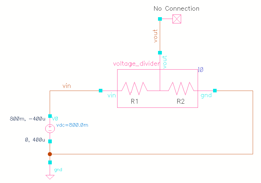
vin, either connectvoutto "noConn" from "basic" library or keep it floating, and ground thegnd. Here’s how it should look:

- Drop in a DC voltage source (we’ll go with 0.8V) at
- Fire up the simulation in ADE Explorer:
- In ADE Explorer, head over to Tool > Calculator and pick vdc. Select the
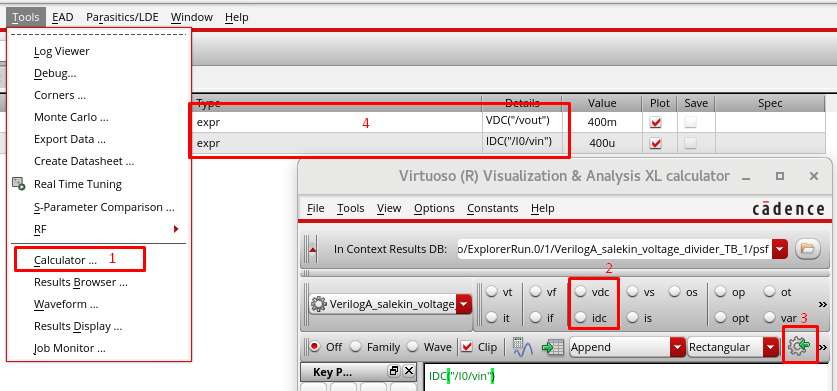
voutnode to create an output voltage expression. Then click on Send buffer expression to the ADE outputs in the calculator to add it to your output list. Do the same for current by choosing idc from the calculator. Here’s a quick snapshot to guide you:

- In ADE Explorer, head over to Tool > Calculator and pick vdc. Select the
- Now, hit Run to start the simulation and check out your results in ADE Explorer. As you’d expect,
voutshould show half of VDD (around 400 mV) if all went well. Success!
Summary for Day 4
Today, we covered how to:
- Set up and use ports and electrical nodes in Verilog-A.
- Simulate a trusty voltage divider circuit in Cadence Virtuoso to confirm voltage division.
Coming up on Day 5, we’ll dive into analog behavior for more complex circuits. Keep up the great work, and get ready for the next step in mastering Verilog-A!
